EE4585 Semiconductor device physics
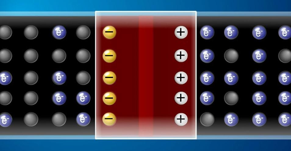
In this lecture first the movement of charge carriers in doped semiconductors under the influence of generation, recombination, drift, and diffusion is discussed. This knowledge is applied to p-n junctions. The current through this junction can be described well by the drift-diffusion model. For a metal-semiconductor junction the model describing the current-voltage relation ship is based the thermionic emission.
The p-n junction is the base for the bipolar transistor. In the bipolar transistor the reverse current of one p-n junction (the base-collector junction) is controlled by the injection of charge carriers from a forward biased p-n junction (the emitter-base junction). Some characteristics, like the Early effect and current crowding, are discussed.
Also another transistor, the MOSFET, is discussed. This device is based on a MOS capacitor to which we will pay attention first. In this transistor the current is led via the source contact through a conductive channel in a semiconductor to the drain contact. The conductivity of the channel can be controlled by changing the bias on the gate contact. Characteristic for this device is that the current-voltage relationship is more linear in contrast to the bipolar transistor where it is exponential.
Following the discussion on ideal MOSFETs, we will then focus on non-ideal characteristics of MOSFETs, like channel-length modulation and short-channel effects. Additionally, we will also pay attention to threshold voltage modification by varying the dopant concentration and MOS scaling. A combination of an n-channel and p-channel MOSFET is used for CMOS devices that form the basis for current digital technology. The operation of a CMOS inverter will be explained. We will explain in more detail how the transfer characteristics relate to the CMOS design.
Finally, we will pay attention to power devices, like power MOSFETs, thyristors, and insulated-gate bipolar transistors (IGBT).
Study Goals
This course aims at a thorough understanding of the physics of semiconductor devices. Students are expected to be able to explain the operation of these devices based on the design and material properties. In addition, they should be able to derive mathematically the most important device characteristics, based on the physics of the device.
Teachers
R.A.C.M.M. van Swaaij
Last modified: 2023-11-04

Details
| Credits: | 5 EC |
|---|---|
| Period: | 0/4/0/0 |